In the Basys Chronicles Episode 1, I started to learn about FPGA programming using Xilinx’s Vivado tool and the Digilent Basys 3 Trainer Board. Now, after a few weeks (okay, time flies; it’s been almost two months), I’ve made some good headway in understanding FPGA architecture and creating some interesting designs that do useful things.
Last time, I followed the directions within the Vivado Udemy course to program the Basys 3 with the provided Vivado seg_display.xpr project. Admittedly, this project doesn’t do much by itself. There’s no meaningful processing of user input, nor interesting visual output. And the course does a good job of teaching you how to use Vivado, but it doesn’t explain what’s going on under the hood – it’s more of a cookbook-style tutorial. I wanted to understand more about the technology fundamentals of how FPGAs work. This is particularly fun, because it’s not only about programming; it also requires a foundation in hardware digital logic design. And for this, I had to tap into some additional resources.
First stop was to www.fpga4fun.com. Although its projects are not designed with the Basys 3 in mind, it does have a lot of good basic FPGA information in one place. Fundamentally, FPGAs are made up of logic cells, interconnects, internal RAM, I/O cells, some dedicated routing/carry chains, and clocks.
Logic cells are composed of lookup tables ("LUTs"), D flip-flop(s) and 2-to-1 mux(es) (to bypass the flip-flops if desired). A LUT can implement any logic function – it acts as a “truth table”. It has typically a number of inputs (four in the drawing below); as an example, one AND gate with three inputs and its output OR-ed with another input would fit in one 4-input LUT:
As of the time of this writing, the biggest FPGA in the world, the Xilinx Virtex UltraScale+ VU19P, holds nine million logic cells. By contrast, the Artix-7 on the Basys 3 board I am playing with has 33,280 logic cells.
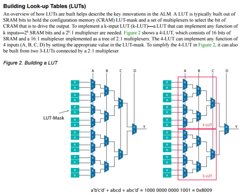
But what’s inside a LUT, and how is it configured to an (arbitrary) logic function? That seems to be a little more complex, and merits some further future research. But, I found this useful diagram while skimming through an Altera (now Intel) FPGA Architecture paper:
Note: the abbreviation ALM in this Figure 2 stands for Adaptive Logic Module. This paper is dated 2006, so I’m sure I can find something more current, but maybe things have not changed that much.
One of the more fascinating aspects of the technology listed above, from my point of view, is the use of JTAG to configure the FPGA. There’s some magic here that defines the FPGA logic functions and circuit connections using the bitstream .bit files generated by Vivado, and that then uses JTAG to scan that configuration into the SRAM bits that make up the configuration memory (CRAM) LUT-mask. There’s a lot of complexity here that is hidden. I’m looking forward to learning more about this.
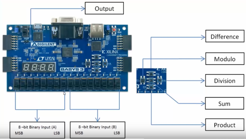
Anyway, that’s it for now in terms of researching the underlying technology. It was time to do something useful with what I’ve learned. I found an excellent YouTube video Getting started with Vivado and Basys3 by Digilent itself, that builds a binary calculator using the switches and buttons on the board, and outputs the decimal results on the seven-segment display. It’s only 16 minutes long, and does a great job of walking a beginner step-by-step through the process. Although it’s no “Hello World”, at least it’s nice to supply some input and see some real output from the firmware.
From below, you can see the binary input is from the slider switches on the board, and arithmetic operation uses the pushbuttons, and the output comes on the display:
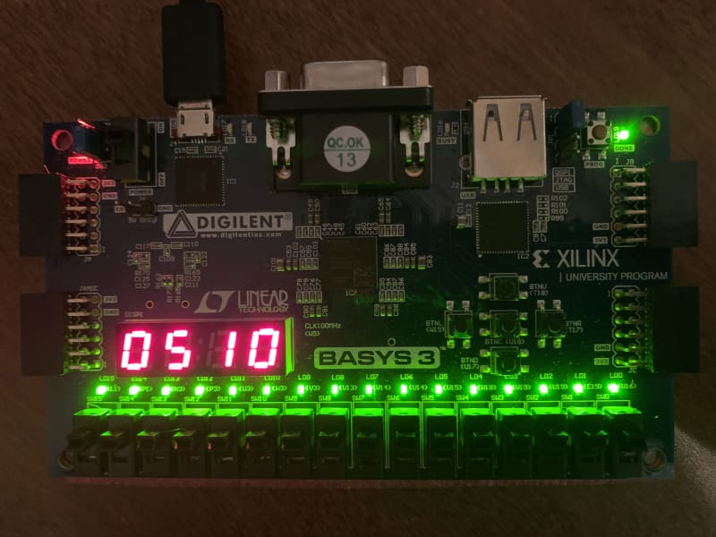
When I put all of the switches in the up position (set to all ‘1’s, so A = 255 and B = 255, and hit the center “Add” button, the correct answer of 510 showed up on the display:
Pretty awesome!
I did find a flaw in the video: Note that I don’t have the Spansion flash on my board, so I was unable to program the SPI flash despite numerous attempts. I finally realized that the flash on my board is from Macronix! I needed a magnifying glass to see the markings. So, I did manage to use the .bit bitstream to program the FPGA, but that program only lasts as long as the board has power. After a power cycle, it goes back to the default Built-In Self Test (BIST) program in the flash, which does some basic hardware verification, as well as cycles the seven-segment display from 0000 -> 9999.
Another small stumbling block in the project (note that the Basys 3 Vivado project is no longer on the Digilent website; you have to download it using Git): at least one of the signals listed in the constraints file Basys3_Master.xdc does match the top module Basys3_Abacus_Top.v: CLK100MHZ in the XDC file does not match clk in the top file. It took me a while to find that.
One final thing I want to say about Vivado: what a powerful tool! It’s a complete development and debug environment, with a ton of features and options. I don’t have anything to compare it against – I haven’t tried the Altera equivalent yet – but it seems to cover all of the bases. My one complaint is the use of the non-intuitive right-click mouse button for a lot of features; it’s easy to miss something if you didn’t know it was there.
Well, that’s it for this week. There’s a lot of interesting things I want to do with the board over the upcoming weeks and months. Some thoughts:
- Program the Macronix QSPI flash with something other than the default BIST firmware, and then put it back (using the GPIO demo in the Basys 3 GitHub).
- Create a “Hello World” program that sends VGA output to a monitor.
- Learn about the MicroBlaze softcore, and have it display some text on the monitor.
- Create a small CPU – maybe even RISC-V? There’s a Git repository that references this: https://github.com/L1ttleFlyyy/RISCVX and its title is RISC-V Processor in a Week! It’s supposed to run on the Xilinx Artix-7. This looks like a complicated little project. And of course, instantiating the softcore is only one step; I’d need to write an assembler or ‘C’ program to get it to do something worthwhile.
- A simpler undertaking might be to create the small CPU that runs the Zork game. There’s a series of videos that start here: Building a CPU on an FPGA, part 1. Watch the first five minutes of this, and you might get hooked. I played Zork on a PDP-11 years and years ago back in school, and it was a lot of fun.
Lastly, I want to give credit to many of the resources I’ve tapped into so far:
There are a lot of good projects referenced on the Digilent website: https://reference.digilentinc.com/reference/programmable-logic/basys-3/start. Examples include a keyboard demo, use of general I/O, and others. They have a few good videos on YouTube, too.
nandland on YouTube: some very cool videos on FPGAs, VHDL and Verilog. If you have a few minutes, have a laugh by watching Why I Hate Karnaugh Maps (note: only true geeks will appreciate this). I sat through many lectures on Karnaugh Maps years ago in a college course, hated them myself, and have never used them since. But, back then they were mandatory learning, and I’m pretty sure I failed that test.
And now, a word from our sponsor: although I may be a newbie, we have a lot of talented engineers in ASSET who have written some pretty powerful RTL for FPGA-based fast flash programming, board test, and other tools. If you want to know more, check out this link: https://www.asset-intertech.com/products/scanworks-fast-flash-programming.


