In a prior blog, I wrote about the JTAG specification’s upcoming 30th anniversary, and reflected on how it has evolved over the years, and the powerful use cases it can be put to. This week, we look at how to secure the JTAG interface, to prevent its abuse by bad actors.
With the emphasis on cybersecurity nowadays, it is more crucial than ever to protect critical system designs from unauthorized access and manipulation. JTAG in particular must be secured, especially since it operates “out-of-band”; that is, separate from and not dependent upon the operation of the overall system. And given its emerging use within Built-In Test (BIT), with the inherent capability of disrupting in-service equipment on a large scale, it is more crucial than ever that potential attacks via JTAG be mitigated.
In general, execution of JTAG private instructions is deemed as a good example of one attack surface. Sometimes (but not always), security-related data/functions are hidden behind undocumented instruction encodings that are not revealed by the Boundary Scan Description Language (BSDL) file of the chip. Attacks via JTAG can look for such “private” instructions in an IEEE 1149.1 implementation. This is relatively easy to do, because the JTAG instruction register has a stated size, and the JTAG documentation (the BSDL file) lists “public” instruction encodings and the size of the instruction register. An attacker only needs to shift in undocumented encodings and pass through UpdateIR (Update Instruction Register) in the 1149.1 state machine to activate undocumented instructions. If the instruction is unused, it generally maps to a BYPASS instruction (where a single shift-capture bit is placed in the TDI-TDO scan path). However, in many cases, undocumented instructions are actually hidden test and debug features, e.g. BIT modes for memory and I/O; manufacturing scan and scan compression modes; or debug modes and functions.
And, of course, any unauthorized system memory access, platform reverse engineering, or insertion of malware/trojans must be protected against.
Given the utility of JTAG, it is common practice to have its port be open on early device samples. The semiconductor suppliers themselves typically use JTAG as a means for silicon validation, to verify early platform functionality. Later, on the early reference boards these suppliers build, JTAG is used for manufacturing structural test and device programming using boundary scan, and various run-control based debug and board functionality validation functions. This is essential to the new product introduction process.
Later, though, production silicon may have the JTAG Test Access Port (TAP) fused off by the chip supplier, as part of its manufacturing process. Obviously, this precludes the valuable use of JTAG by its system OEM customers.
Presuming the device TAP is left open, system designers and manufacturers may try to “lock down” the JTAG interface to prevent unauthorized intrusions at the board level. Clearly, it is necessary to secure JTAG at the chip-level, and at the board-level. Let’s look at these mitigations.
Chip-Level Mitigations
For production parts that will deploy to end users, the most straightforward approach for semiconductor suppliers is to entirely disable JTAG access. This is often accomplished by fusing off the TMS signal (permanently placing the JTAG finite state-machine in the Test-Logic-Reset state):
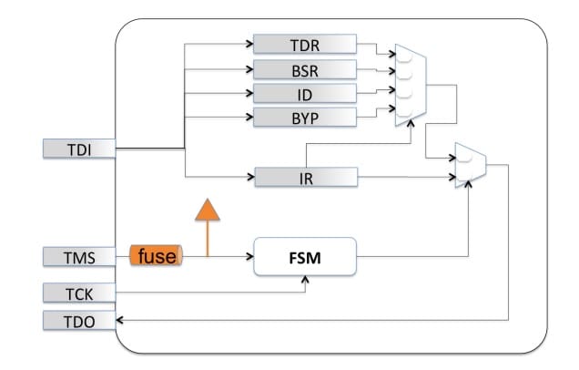 But in this instance, all JTAG functions are disabled—even public functions for board test and software development debug functions become unavailable. Because the JTAG port is often necessary for board/system test, debug, device programming, and validation, this is unacceptable. Again, the problem here is, if you turn off JTAG, what happens if you want to turn it on again? Suppose field failures start to emerge on a product line, and JTAG-based debug is the only access mechanism able to triage the problem? How about turning on some embedded tools within the chip, while keeping others secret? It seems that a secure key system, combined with a multi-factor challenge/response, would be one way to “have our cake and eat it too”. In other words, to have a production part naturally be in a “locked” state, and relatively immune to attack, but have some of its instrumentation unlocked in situations where it is critical to have some valuable debug or test engine execute for root-cause analysis.
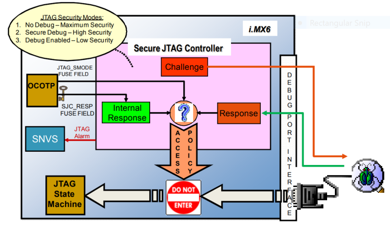
A more flexible approach is as used by NXP for the i.MX 6 series family of applications processors. The i.MX6 series System JTAG Controller (SJC) provides a method of regulating JTAG access. The three JTAG security modes available are:
|
Profile |
Description |
Test Access |
Debug Access |
|
JTAG Disabled |
Highest level of JTAG protection. All JTAG features are disabled. |
Permanently blocked. |
Permanently blocked. |
|
Mode 1: No Debug |
Maximum security. All security sensitive JTAG features are permanently blocked. |
Always available. |
Permanently blocked. |
|
Mode 2 (a): Secure JTAG (without SW enable possible) |
High security. JTAG use is regulated by secret key-based authentication mechanism. |
Always available. |
Available only upon satisfactory response to the invoked challenge. |
|
Mode 2 (b): Secure JTAG (with SW enable possible) |
Option for flexibility in Secure JTAG mode. JTAG use is regulated by software-accessible JTAG Debug Enable (DE) bit. Software access to JDE can be blocked until next reset by write-once LOCK bit. |
Always available. |
Available as above; or on un-blocked software write to HAB_JDE bit. |
|
Mode 3: JTAG Enabled |
Low security. JTAG always enabled. |
Always available. |
Always Available. |
Test features include Scan/boundary scan, MBIST (Memory Built-In Self Test, excluding modes to output memory contents), Phase-Locked Loop (PLL) BIST, BIST monitor mode, and visibility to some status bits. Debug features include run-control and trace.
These JTAG modes are configured using One Time Programmable (OTP) eFuses which are burned after packaging using the NXP Manufacturing Tool. In addition to these three modes, there is an option to disable the SJC functionality entirely. The fuse burning is an irreversible process; once a fuse is burned it is not possible to change the fuse back to the unburned state.
Presuming Secure JTAG is enabled, the challenge-response mechanism is the responsibility of the system owner. Challenge values are the “Device Unique ID” that is programmed into the eFuses and unique for each IC. The secret response key is also programmed into an eFuse, and no host software can read it. In the overall JTAG flow, the challenge key comes out TDO, the host test/debug application generates the response key, which is shifted back in on TDI, and then Secure JTAG either authorizes access or locks the port:
Key management is left to the system owner. The response keys for each part can simply be identical, can be maintained in a database, or algorithmically generated. Of course, if the response key becomes known, from a database compromise or algorithm exposure, for example, the mechanism is no longer secure.
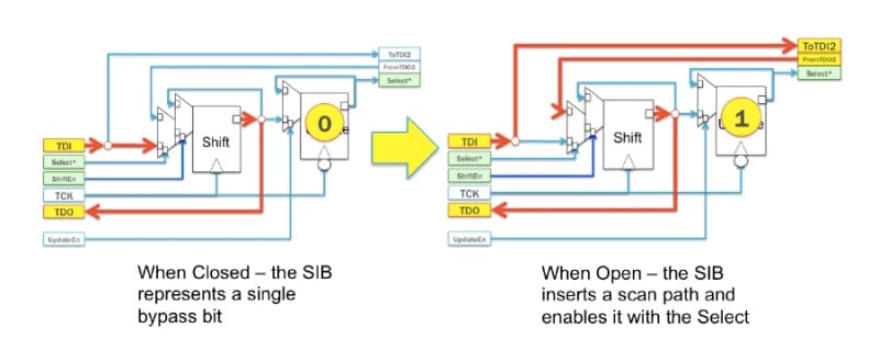
A perhaps more flexible mechanism at the chip level for such an implementation has been documented by ASSET and Southern Methodist University. Built within the IEEE 1687 “Internal JTAG” (IJTAG) specification is the concept of a variable-length scan chain, necessary to provide standardized access to various (could be hundreds or thousands) of “embedded instruments” within the chip while providing meaningful access times and concurrency. This network of instruments is placed behind segment insertion bits (SIBs) that control access to different scan chains for different instruments:
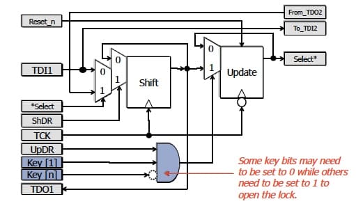
This paper proposed a method for hiding instruments in an IEEE 1687 network utilizing a “locking” segment insertion bit (LSIB) that can only be opened when pre-defined values, corresponding to a key, are present in particular bits in the chain:
Also introduced in the paper were “trap” bits, that can further reduce the effectiveness of brute force attacks by permanently locking an LSIB when an incorrect value is written to the trap's update register. Only a global reset will then allow the LSIB to become operable again. IJTAG-based honeypots therefore may make an attacker incorrectly think he or she is making progress, only to have to start over.
Of course, providing these mitigations at the chip-level requires key management, inclusive of device digital signing and supply chain key management, as with the NXP Secure JTAG implementation.
Board-Level Mitigations
Regardless of what is implemented at the device level, board designers have a responsibility to protect the JTAG interface at a PCB level. This is often part of an overall system security strategy, to ensure that any given in-service platform is not compromised in any way by bad actors. Often, JTAG headers are physically removed from PCBs at the end of manufacturing production. Steps are taken to remove physical access to the five JTAG wires and prevent the connection of an external JTAG agent (typically a debugger); this can be done with jumpers, or access is simply designed out. The challenge remains of continuing to provide JTAG access on production systems, on an at-scale basis, should test or debug applications need to be executed on the platform to address NFF, materiel availability, and root-cause issues.
This is obviously a very broad topic, and the subject of much research. Let’s focus on situations where JTAG is used for out-of-band BIT on high-availability systems. In these environments, JTAG is always available for test and debug, and access is controlled by both a service processor and a separate trusted device. That access to the JTAG scan chain must be secured without necessarily modifying the integrated circuit components and physical connectivity of the chain.
Mitigations must consider the need to not only prevent unauthorized access, but also to detect if it should happen. The two major attack vectors are the JTAG interface itself, and any and all components that are part of the JTAG chain, particularly the out-of-band service processor itself. Let’s examine these two attack vectors, and look at some mitigation approaches for them.
Attacking the JTAG chain itself
Security through obscurity is often considered an inadequate mechanism of preventing unauthorized attacks. In other words, the goal is not just to prevent attacks, but to detect them, and mitigate against them. As it relates to JTAG, the presumption is that at some point a bad actor obtains access to the board JTAG chain, either via direct physical access, or via a device that has access to the chain. As such, the hardware root of trust must be capable of detecting the intrusion, and disabling access pending further analysis.
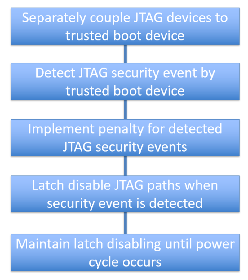
One approach to this is as documented within Patent No. US 9,810,736 B2. Board scan chains are secured via a trusted boot device, that “sniffs” the chains for unauthorized activity. The JTAG paths on the secure trusted boot device are latch disabled by default. When JTAG is needed for test or forensics, it is only enabled for a predefined period of time. A security event is triggered in the event of an intrusion, or if JTAG activity exceeds the allotted time; and a system power-cycle is needed to subsequently re-enable authenticated JTAG enable requests. The overall flow looks like this:
A key defensive strategy is to ensure that all devices that have the potential to master a board’s JTAG chain must be part of a hardware root of trust. In other words, they must be trusted not to attempt to master the JTAG chain and put it to nefarious purposes.
Service processors responsible for system management, and in particular those who have access to main board functional devices through JTAG, must be made resistant to attack. Especially given that many of these may contain programmable logic (firmware) that could potentially be corrupted, establishing a silicon root of trust, such that all boot code of such devices is always verified, is essential. Protecting the JTAG chain is but one of the outcomes of securing the firmware and bootstrap code of such devices. There are numerous solutions in place and underway that implement these protections, among them:
Project Cerberus
The Project Cerberus Security Architecture is a well-documented implementation. Within this specification, a hierarchical Root of Trust is established. At the foundation is the Cerberus microcontroller, and it and each active component (that is, devices that boot to an operational state before the platform’s host processor completes its initialization and becomes capable of challenging the devices) are roots of trust for their own functional domains.
The Cerberus architecture provides for hardware enforced platform security, actively controlling power-on of each active component and the host system. All device boot is secured, attestation done to prevent/detect corruption, firmware updates controlled, and recovery implemented where possible.
Titan
Google Titan is an architecture that also uses a security chip designed to protect servers from firmware-based rootkits and other malware-infecting firmware. Titan is a key element in Google's security and allows the company to boast that security for its Google Cloud Platform services goes to the hardware root of trust level.
The Titan chip comprises several components: a secure application processor, a cryptographic co-processor, a hardware random number generator, a sophisticated key hierarchy, embedded static RAM (SRAM), embedded flash and a read-only memory block. Titan communicates with the main CPU via the Serial Peripheral Interface (SPI) bus, and interposes between the boot firmware flash of the first privileged component, e.g., the BMC or Platform Controller Hub (PCH), allowing Titan to observe and validate the boot firmware as it loads and executes, from the very first instruction.
Like Cerberus, Titan verifies its own identity upon power-on, and also that of active components. Titan also supports continuous monitoring on SPI buses for illegal activity.
So, that’s it for now. I hope that this has presented a high-level overview of a complex subject. It takes a rigorous design approach to secure the JTAG interface on designs. But, given the value of JTAG, it’s worth it.



One Response
I don’t see people talk about the non-intrusive aspects of JTAG that are important for NFF testing. SAMPLE is a powerful tool that can still be used for test analysis, albeit far limited to what can be done with EXTEST. One is able to detect changes on inputs to confirm an open is not existing, for example. Similar state capture of internal registers is extremely important and not impacting device operation. These could be left intact as partial fused configurations by fusing the select lines of other registers as a simple implementation.