In Episode 2, I said we would be looking at the Multiplex IO (MIO) next, but before we dive into looking at the MIO, I have a desire, call it a nagging question, to look at the code in the QSPI. So I’ll divert this episode to that endeavor and return to the MIO initialization as soon I have an answer to my nagging question.
To chase this rabbit, in this episode, we will examine the code required to configure the QSPI controller, and download some code into the OCM or DDR, and finally perhaps write a macro to dump the QSPI memory. But first the backstory.
So far, we have booted the FSB/Linux for board operational checkout, connected the ASSET SourcePoint C/C++ debugger via JTAG in Zedboard Chronicles Episode One. In the second Chronicle, we initialized part of the Xilinx Zynq-7000 PS via macros so we could interrogate or use the on-board DDR.
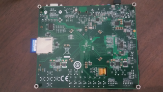
Let’s start with a discussion about accessing the SPI flash device. The SPI device on the Zedboard is a S25FL256SAGMFI00 according to the schematic. On the Zedboard schematic, I noticed that this is not your ordinary single channel SPI flash memory. To be certain that I had the same SPI device populated on my version of the Zedboard, I had to physically locate the device. I found it located on the back of the Zedboard next to the SD slot. Looking at the device marking, I see that it is a Spansion device next to the SD slot in Figure 1:
Unless you have been keeping up with the silicon mergers and acquisitions, you would not know that Spansion is now Cypress. The reason for the goose chase is, we need a data sheet to understand a little about the SPI device, and to tell us more about the other three serial lines. We need to chase down a Cypress data sheet. There are many data sheets provides on the net, just look for one with the part number below.
According to the Cypress data sheet on the 25FL256SAG, we see that this is a 256Mbit SPI flash memory.
This family of devices connect to a host system via a Serial Peripheral Interface (SPI). Traditional SPI single bit serial input and output (Single I/O or SIO) is supported as well as optional two bit (Dual I/O or IO) and four bit (Quad I/O or QIO) serial commands. This multiple width interface is called SPI Multi-I/O or MIO. In addition, the FL-S family adds support for Double Data Rate (DDR) read commands for SIO, DIO, and QIO that transfer address and read data on both edges of the clock. Further reading we find….
Traditional SPI single bit wide commands (Single or SIO) send information from the host to the memory only on the SI signal. Data may be sent back to the host serially on the Serial Output (SO) signal. Dual or Quad Output commands send information from the host to the memory only on the SI signal. Data will be returned to the host as a sequence of bit pairs on IO0 and IO1 or four bit (nibble) groups on IO0, IO1, IO2, and IO3. Dual or Quad Input/Output (I/O) commands send information from the host to the memory as bit pairs on IO0 and IO1 or four bit (nibble) groups on IO0, IO1, IO2, and IO3. Data is returned to the host similarly as bit pairs on IO0 and IO1 or four bit (nibble) groups on IO0, IO1, IO2, and IO3.
That explains the extra serial lines. In section 3.2 of the Cypress data sheet, there is a lengthy discussion about command protocol; enough already!
Let’s see what the Zynq can do to manage this “simple” SPI device. Chapter 12 of the Zynq-7000 TRM is dedicated to the Quad-SPI Flash Controller, only 25 pages to master. Still looking for shortcuts, I see in the section labeled Address Map and Device Matching for Linear Address Mode: When a single device is used, the address map for direct memory reads starts at FC00_0000 and goes to a maximum of FCFF_FFFF (16 MB).
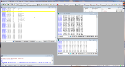
Eureka! We have a starting address for the SPI. Now to open a memory view of the device, and dump the contents. Dumping the memory contents is shown in Figure 2:
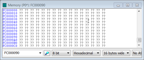
Doing so, I get all question marks (Figure 3) and I have lost control of the target? What happened?
I should have listened to the hint I left at the end of the Zedboard Video Chronicles Episode 2 or read a little more in the data sheet and TRM. Alarms should have sounded, when I read that there was a command protocol to access the device. But why did the target lose JTAG run-control?
The attempt to read from a region that can’t be read would generate an exception, and the processor would follow the exception path. Chasing down this exception code flow will be left for another chronicle but that would likely explain why JTAG control was lost.
Actually I knew this would happen: you can’t access a serial device that needs a controller to execute the commands to get the data read from the device, by simply opening a debugger memory view, without setting up the controller first. However there is a way to dump the contents of the QSPI.
Let’s start by looking at for QSPI read information in the TRM. As stated earlier, Chapter 12 of the TRM is dedicated to the QSPI controller. In section 12.3 there is a high level programming guide that show the steps required to get access to the flash memories.
Example: Start-up Sequence
1. Configure Clocks. Refer to section 12.4.1 Clocks.
2. Configure Tx/Rx Signals. Refer to section 12.5.2 MIO Programming.
3. Reset the Controller. Refer to section 12.4.2 Resets.
4. Configure the Controller. Refer to section 12.3.1 Configuration.
Now, either configure the controller for linear addressing mode (section 12.2.5 Linear Addressing
Mode) or configure the controller for I/O mode (section 12.3.3 Configure I/O Mode and section
12.3.4 I/O Mode Interrupts).
As we can see, there are a number of steps, and these steps are broken down into subsequent steps. We need to determine how to access this flash either in linear or I/O mode. We will be using the linear mode. There are some basics that need to be covered regardless of the mode we choose, and in the TRM there is a basic configuration. The values to program into the qspi.Config_reg register are shown in Table 12-3, page 345.
Example: Write to the qspi.Config_reg register
Configure the controller. Write to the qspi.Config_reg register.
a. Set baud rate, [BAUD_RATE_DIV].
b. Select master mode, [MODE_SEL] = 1.
c. Select flash mode (not Legacy SPI), [LEG_FLSH] = 1.
d. Select Little Endian, [endian] = 0.
e. Set FIFO width to 32 bits, [FIFO_WIDTH].
f. Set clock phase, [CLK_PH] and Polarity, [CLK_POL].
2. If baud rate divider is 2, then change default setting. If the qspi.Config_reg[BAUD_RATE_DIV]
is set to 0b00, configure the qspi.LPBK_DLY_ADJ (loopback delay adjustment) register with the
following settings:
a. Set to select internal clock. qspi.LPBK_DLY_ADJ[USE_LPBK] = 1.
b. Set the clock delay 0. qspi.LPBK_DLY_ADJ[DLY0] = 0b00.
c. Set the clock delay 1. qspi.LPBK_DLY_ADJ[DLY1] = 0b00.
And finally the configuration of the Linear Addressing Mode.
Example: Linear Addressing Mode (Memory Reads)
The sequence of operations for data reads in linear addressing mode is as follows:
1. Set manual start enable to auto mode. Set qspi.Config_reg[Man_start_en] = 0.
2. Assert the chip select. Set qspi.Config_reg[PCS] = 0.
3. Program the configuration register for linear addressing mode. Example values are shown in
Table 12-3, page 345.
4. Enable the controller. Set qspi.En_REG[SPI_EN] = 1.
5. Read data from the linear address memory region. The memory range depends on the size
and number of devices. The range is from 0xFC00_0000 up to 0xFDFF_FFFF.
6. Disable the controller. Set qspi.En_REG[SPI_EN] = 0.
7. De-assert chip select. Set qspi.Config_reg[PCS] = 1
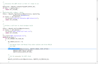
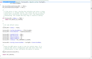
Now it is time to see what Xilinx has provided for setting up the QSPI on the Zedboard. I’m always looking for time savings. In the Xilinx SDK, the BSP has support for initializing the QSPI controller and a driver. My expectation is to learn enough to not only read from QSPI but to program QSPI. Looking thru the driver I see at least two functions that need to be used in my code. The first is XQspiPs_CfgInitialize and XQspiPs_SetOptions these are the functions that setup the configuration register for the QSPI controller and the send and receive buffers. The BSP follows the steps exactly if you spend enough time walking through the code. So here is a code fragment (Figure 4) that does part of the task.
Diving into the XQspiPs_CfgInitialize routine, we see that here is the instance of setting up the buffers, send and receive, and the base address of the QSPI configuration register shown in Figure 5.
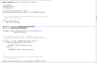
In the XQspiPs_SetOptions call from above (Figure 4), drilling deeper, into this function below, we see that this is where the QSPI is being set up for Linear mode and that was one of the objectives of this episode. Shown below in Figure 6.
Ok, enough of the code walk. The next step is to complete the programming application, where we will provide support for the following features: Erase Device, Erase Sector, Blank Check, Program Sector, Program Device, Verify Sector, Verify Device, Blank Check Device, and Dump Device. With the code complete and debugged, we can now configure the QSPI controller and then read the QSPI contents.
After loading the elf object module, with code and symbols, into the target from the SourcePoint debugger. We can simply type main into the code view and start the configuration of the QSPI controller by executing the code. As mentioned earlier, this code has a number of options for dealing with the QSPI flash. We will concentrate on the Dump Device control.
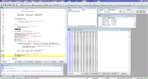
The way the BSP behaves is to setup a ReadBuffer, and then enable the QSPI controller to provide commands necessary to interact with the SPI device. The buffer size in the BSP is smaller than the whole SPI device. In the code segment below, that we have executed, the code reads the content of the QSPI and fills the ReadBuffer several times. Because we what to see the total content of the SPI, we copy the contents of this buffer to a larger buffer on each readbuffer fill pass. This larger buffer is capable of handling the entire contents. I have stopped the execution at the point, where the last buffer was copied to larger buffer (DDR space) Figure 7.
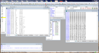
By looking in a memory view (shown in Figure 8), hex data format, of the buffer that contains the whole SPI image, it is difficult to assess if this is code or data. By using the code view, and selecting the buffer address 0x18000000, we see that this could be code but the first few entries are not what we would expect.
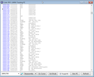
By scrolling down in the memory view, I noticed that there is potential code at offset 0x1700 from the base of the buffer (Figure 9)
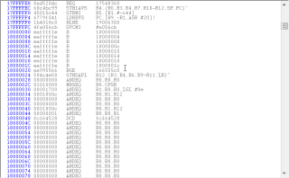
Now opening a code view (Figure 10) at that address, the data seems to be reasonable. The first few entries could be an exception vector table. Not really sure what we have located.
So now we have a view of the QSPI or at least the contents of the QSPI. Which answers my nagging question. My next challenge is to find the source to the contents of the QSPI which should be the First Stage Boot Loader (FSBL). I’m not as much into assembly code now as I once was years ago. Also, I want to attempt to create a macro that does the setup of the QSPI controller and opens the memory view from a single click of a button. But that will be left to another Zedboard chronicle.


