
Recently I read a posting from a well-known In-circuit Test (ICT) vendor defending the use of test pads on high-speed signals. I found this message to be rather amusing, since the prevailing wisdom is to avoid these to prevent signal integrity issues.
The posting went something like this:
We have done some simulations that indicate that test pads can still be used for high speed signals if they are properly designed and added correctly to the PCB. The test pad must be on the signal etch without a stub connecting the etch to the pad. Also, there should not be a via connecting the etch to the test pad.
The results indicate that a 35 mil pad on a 5 mil wide etch is OK for 10Gb/s with 30ps rise/fall times.
If there is still a worry about test pads, the test pad can always be "compensated" by removing some of the reference plane below the test pad to diminish the additional capacitance that might otherwise occur. If the test pad per-unit capacitance and inductance is nearly equal to the per unit capacitance and inductance of the transmission line's etch, then the test pad will have no net negative effect to the signal transmission.
The first paragraph correctly highlights some of the pitfalls of putting test pads on high-speed signals. The trend these days is to route traces for high-speed signals on inner layers of the PCB – in which case it is only possible to add a test pad by way of a via, which is not a good idea.
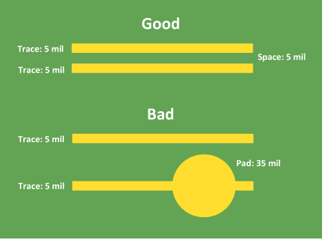
Even assuming that the nets are on an outer layer, you certainly don’t want to have a stub to a test pad on one of them:

After this though, their logic collapses. If the signal is on an outer layer, it’s not possible to place a 35 mil test pad directly on a 5 mil wide trace without creating a PCB routing nightmare. Differential signals are intended to be closely coupled, and the radius of the test pad will create additional routing constraints where they are already likely to be over-constrained:
And the suggestion to remove some of the reference plane seems bizarre – imagine it resembling a curious form of Swiss cheese, to the detriment of ALL signals (not just the ones being test-pointed). This of course assumes that CAD tools are available which can perform this function.
Finally, the posting starts with the clause “We have done some simulations…”. This by itself should raise major concerns. Simulations are only approximations of reality. Show me some empirical evidence backing up these statements, and I might believe it. For more on the subject of simulation versus reality, read Glenn Woppman’s column in our June issue of Connect.
Board test engineers need to proactively plan to test high speed signals using non-intrusive technologies such as boundary scan, processor-controlled test, and other on-chip I/O instrumentation such as Intel® IBIST.