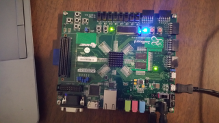
I was challenged by my colleague, Alan Sguigna, author of The Minnowboard Chronicles, to write about my experiences with the Zedboard. We recently purchased a Zedboard from AVNET to better understand the capabilities of the SoC. The Zynq is unique in that not only does it contain a dual-core ARM® Cortex™ A-9, referred to as the processing system (PS), but also the Xilinx programmable logic (PL).
It is one thing to read the marketing or technical data from a website, but it is a whole lot more fun to get your hands on the real thing.
Our desire was to see if SourcePoint, ASSET’s best-in-class ARM software debugger, would simply plug in and work; after all the SoC core is the ARM Cortex A-9 and the debugger supports this core. We should state that all targets require a target configuration file to configure the SourcePoint debugger to deal with the CoreSight™ complex which comprises debug and trace control.
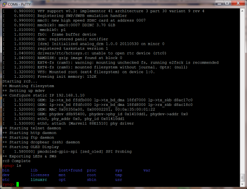
In addition to the challenge from my colleague, my desire was to better understand the use model and the tools available to support this powerful SoC. The first test was to connect the UART interface to the Windows 7 platform using PuTTY as the communications application. Finding the Cypress driver for windows was a little challenging but after installing, launching, and configuring, we are able to see the board boot the Linux kernel. Notice that the Mode boot select was set to QSPI boot.
We now know the board is booting properly, and can proceed with the experiments. The boot process of the Zynq is quite interesting as it is a multi-stage boot process. First is the hardware part of the boot process, this includes the power supply ramping, clocking, resets, pin strap sampling, and optionally enables the PS PLL clocks. The PS then begins executing the BootROM code in the on-chip ROM to boot the system. The sampling of the mode pins is how the PS determines where to go next in the software boot flow. With the mode pins set for JTAG mode, the BootROM does some minimal system configuration and enables the JTAG interface. We won’t go into the details, but there are two JTAG controllers in this device. One is the DAP which allows access to the PS and the other is the PL JTAG interface.
Plugging a debugger, that uses JTAG to communicate, into a new target is stepping into the unknown. Is the hardware configured properly i.e. do we really have JTAG access? Are the watchdog timers turned off? Other hardware interrupts that could affect communications? Then what about the firmware? Off into the unknown…
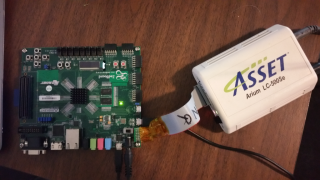
Next step involves plugging the SourcePoint probe into the Zedboard and see how the system handles the JTAG boot control. The mode selection jumpers need to be change to support the JTAG slave boot.
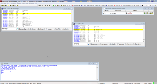
The plugin was successful and both cores (see below) are in a wait for event loop. With SourcePoint, there is a view called the ViewPoint that allow the user to switch between each of the core and also provides independent core control of running, resetting and various forms of stepping. The code views shown below are locked to show the code executing on each core. The code view defaults to tracking the viewpoint context. Examining the code below, we can see that the wait for event for core 0 is executing between 0xfffff20 and 0xffffff28 while the code for core 1 is executing between 0xffffff2c and 0xffffff40. From this address range we can see that we are in OCM. 
So now what to do? Can we read and write memory? On-chip memory (OCM) should be controllable. Can we read and write registers? After checking out the ability to control both the OCM and the registers, we have a bit of a dilemma or decision to make about what is next.
For the board to load the First Stage Bootloader (FSB), we need to decide where the bootloader will reside: QSPI, SD or other. We also need to check out the DDR as this will be the ultimate destination of the FSB or bare-metal application. We also need to configure the MIO. We need to initialize the MIO, the QSPI controller, the PLL and the DDR controller. Not necessarily in that order. So we either load code into the OCM that will allow us to do more work, a loader agent or flash agent, or we configure the SoC by writing to the control registers of these various controllers using the SourcePoint debugger.
If you have looked at the Technical Reference Manual (TRM) for the Zynq 7000, all 1,863 pages, you are struck with the magnitude of the coding effort to initialize this SoC depending upon target design and the SoC SKU. We will start with the MIO interface. Writing the C code to configure each bit or group of bits within the SoC Register space is a task, then you need to debug it. There is a better way or at least a short way to begin the configuration of the SoC components. The shortcut eliminates the edit, compile, link load and debug loop, at least for now. SourcePoint provides a C like macro language that can be loaded directly to setup these control registers. Xilinx SDK provides a Tcl file that accomplishes the same task. We converted this Tcl script into a SourcePoint macro. By loading the ps7 macro we can initialize the MIO, PLL, Clocks, DDR, and the peripherals. With this initialization we can now load software executable (elf files) into DDR memory and use the symbolic data from the elf file to increase our development pace with better comprehension.
In the next episode we will cover using the macro language and configure the DDR.
If you want to know more about SourcePoint, please feel free to visit our website here.
There’s an excellent video of the GUI which shows the ease-of-use and power of the tool on that page. You can also request a live demo here.


