Boundary-scan test is used commonly on manufacturing lines with a “benchtop” tester, complete with cables, fixturing, hardware probes, and so on. What are the pros and cons of embedding this technology in-situ?
Boundary-scan test continues to be used as a powerful technology for detecting structural defects on printed circuit board assemblies. As such, it has found a niche on many manufacturing production lines, either in conjunction with In-Circuit Test (ICT), or as a replacement thereof.
But as with all such “benchtop” or external JTAG-based technologies, there is a cost associated with accessing the JTAG control test pins on the printed circuit board. Hardware controllers or probes are needed to host the JTAG master or scan engine functionality. Cables and connectors are needed to make the physical connections to the unit under test. PCs are needed to host the boundary-scan test application. And, of course, in some cases, access to necessary board header(s) may be entirely precluded, due to heat sinks, shielding, or some other obstruction; or the board may be loaded within a chassis within a system, and no access is possible.
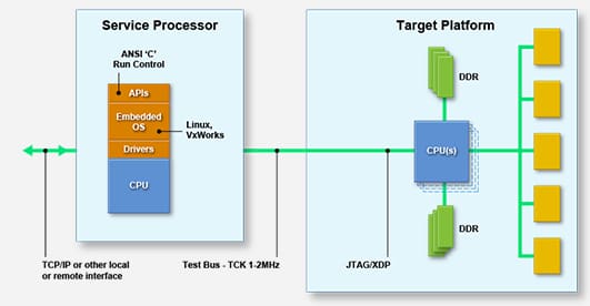
Embedding boundary scan in-situ is one solution to this limitation. The JTAG master functionality and required boundary-scan action players are loaded into an on-board service processor, which is given direct access to the PCB’s scan chain. On an Intel-based server design, a Baseboard Management Controller (BMC) performs the service processor function, and the topology looks like this:
The technical challenge associated with this approach revolves around embedding the technology within the BMC firmware, and making the appropriate design changes on the board to concatenate chains to get the highest possible test coverage. The latter is needed, even for benchtop testers; and the effort associated with including boundary scan within a BMC firmware image can be ameliorated by making it “non-resident” – that is, downloaded dynamically at test time, and then removed subsequent to completion of the test.
The benefits of embedded boundary scan are, of course, significant. It can be used at all stages of a product’s lifecycle – prototype, new product introduction, volume manufacturing production, manufacturing debug, HALT/HASS testing, field repair, and failure analysis. It requires no external cabling, hardware controllers, or fixturing. Tests can be run at the push of a button, and even be built into an in-system test or diagnostic suite to capture root cause forensics at a customer’s premises. And true “system-level” tests can be run even in systems where physical access is impossible.
For a Case Study of how a customer used embedded boundary scan to detect Intel QuickPath Interconnect (QPI) defects on a board in an environmental chamber, see our eBook, JTAG Diagnostics for Intel QPI Structural Defects.


