As we’ve covered in some previous blogs, the differential,
AC-coupled nature of PCI Express allows this bus to be somewhat self-healing,
whereby some structural defects will allow the bus to transparently run, albeit
at a degraded performance. Due to this, these short-circuit and open-circuit
defects may be completely masked from conventional functional test. But such
defects are important to detect, because they will affect the throughput of the
port. Boundary scan can be used to detect these defects, subject to the
implementation of IEEE 1149.1 and IEEE 1149.6 in the chips.
As we saw summarized in Structural Defects on High-Speed Serial I/O – Part 3, some
shorts and opens will cause a link to run at a degraded performance, with lower
margins and higher bit error counts. For example, a single open due to a
missing capacitor, or a short between Tx1+ and GND or between Tx1+ and Tx2+
will have this effect. That’s why these defects are so nefarious; they may be
invisible to conventional manufacturing functional or system test, and then
only cause problems subsequently out in the field. But, it would seem that
boundary scan should be able to detect such defects with 100% reliability,
right?
Well, the answer to that question is highly dependent on the
implementation of IEEE 1149.1 and 1149.6 (AC-JTAG) within the associated chip.
Let’s first look at an example by considering a processor chip with PCI Express
gen3 out to an unpopulated PCI Express connector:
It is worthwhile to note that the PCI Express specification
requires that the AC coupling capacitors be as close as possible to the
transmitter buffers, so they will be on-board the printed circuit board where
the processor resides in this diagram. The other coupling capacitors for the
processor receive buffers will be on the PCI Express add-in card.
Also, since the PCI Express slot in this example is
unpopulated, the two Rx1+ and RX1- lanes are open; that is, they are in a high-Z,
or tri-stated high impedance condition. In other words, they are not being
driven to any defined logic level.
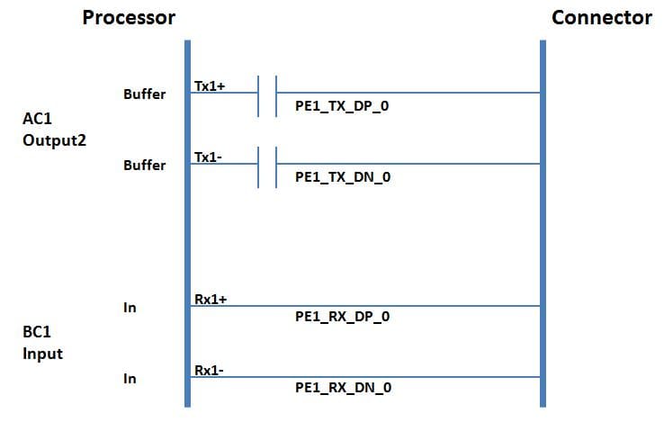
Now let’s look at an excerpt from the hypothetical BSDL file
for this processor, for PCIe lane 1:
(from the Port statement):
PE1_RX_DN_0; in bit;
PE1_RX_DP_0; in bit;
PE1_TX_DN_0; buffer bit;
PE1_TX_DP_0; buffer bit;
(from the port grouping statement):
“Differential_Current ((PE1_TX_DP_0,
PE1_TX_DN_0)),”&
(from the boundary register statement):
“121 (BC_1 PE1_RX_DN_0, input, x ),”&
“122 (BC_1 PE1_RX_DP_0, input, x ),”&
“123 (AC_1 PE1_TX_DP_0, output2, x ),”&
(from the AIO pin
behavior statement):
“PE1_RX_DN_0 : HP_time=8.0e-9 ;”&
“PE1_RX_DP_0 : HP_time=8.0e-9 ;”&
“PE1_TX_DP_0 ;”&
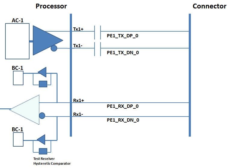
What’s going on inside the processor chip, per this BSDL,
can be seen diagrammatically:
There are several useful things to note here regarding a
static DC-only level-sensitive boundary scan implementation for IEEE 1149.1:
- The positive and negative transmit nets are
driven by a two-state output-only buffer, so these nets can drive but cannot
sense. So shorts between these two nets could not be detected. Also, with DC
stimulus only, opens on these nets cannot be detected (of course, these nets
are “open” because there are capacitors on the nets which in turn connect to an
open connector). - Shorts between either of these two transmit nets
and a separate net with a bidir cell could be detected. - The receive cells are input-only and can’t
drive. - Since the receive cells are open and high-Z,
these nets don’t have a known state at all test steps, so shorts between these
nets and any other nets are not covered. And of course opens cannot be detected
because these nets are explicitly open.
So the boundary scan test coverage on PCIe is categorized as
“Class 3”: some coverage on stuck-at 0 or 1, but not much else.
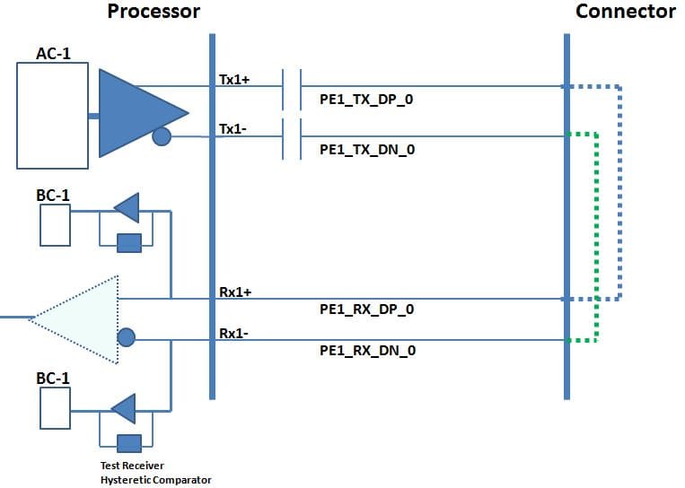
Things get interesting when we put a passive loopback card
(which connects transmit nets to receive nets) and use some of the features of
IEEE 1149.6 (AC-JTAG) to these nets. This gives us shorts and opens test
coverage on both the component side and connector side of the bus.
Note that Tx1+ is now looped back to Rx1+, and Tx1- is
looped back to Rx1-. So shorts between these nets are now explicit as part of
the loopback, and they will not be detected by boundary scan. But, as we’ve
seen from our previous blogs, these defects will be detected by either
processor-controlled test or HSIO using an active loopback card.
Any opens on either the board, connector or add-in loopback
card due to missing BGA balls, connector plated through-hole issues, etc. will
be detected as normally by IEEE 1149.6.
Of course, if there are shorts between Tx1+ and Tx1-, or
between Rx1+ and Rx1-, no signal will go out on these differential pairs, and
the lanes will fail. A clever 1149.6 interconnect test which detects edges on
the receive side of the looped pair will now see the lack of an edge, and
isolate the fault.
You can see that using edge detection on the virtual
receivers to the BC_1 cells using EXTEST_PULSE or EXTEST_TRAIN will allow us to
detect and diagnose shorts between Tx1+ to Rx1+, Tx1+ to Rx1-, Tx1- to Rx1+ and
Tx1- to Rx1-.
So a prescribed boundary scan test sequence for PCI Express
would consist of:
- With nothing in the PCIe slot, run an 1149.1
static test to get Class 3 coverage on shorts. - Insert a passive loopback card into the PCIe
slot, and then run an 1149.6 test for opens and shorts.
The only defects that might escape from this methodology, of
the Tx1+ to Rx1+ and Tx1- to Rx1- type, could then subsequently be detected
with either processor-controlled test and/or HSIO.
For more information on the use of boundary scan technology for high-speed nets, check out
our IEEE 1149.6 boundary scan tutorial. For more information on
processor-controlled test or HSIO, check out our white paper on Non-intrusive Board Test.


2 Responses
You might not have chosen the best example for AC boundary scan.
I had to test PCIE device that had a built in pattern generator that could be set up using an I2C interface and a “certified PCIE Loopback”. This allowed a 5 and 10 Gig “at speed” traffic test.
Granted BS would give pin fault diagnosis, in my case there was only 1 JTAG device on the board.
The above is a very rare instance, typically EVERY board we test has some AC boundary scan, and we make extensive use of loopbacks.
The AC-JTAG example used in the blog is from a commonly-used processor, so it’s always worthwhile to very carefully examine the BSDL for the device to determine the level of test coverage available. You don’t always get the test coverage (i.e. Class 3 vs. Class 1) that might be expected.
Further, the amount of coverage obtained from the “certified PCIe loopback” depends on the nature of this test. We have seen some structural defects (such as a missing capacitor) which are very difficult to detect (i.e. require very long test times) at nominal time and voltage using at-speed traffic tests. This is described in my blog at https://blog.asset-intertech.com/test_data_out/2013/03/structural-defects-on-high-speed-serial-io.html. The defect can be manifested more quickly by margining the traffic (varying the voltage/time offsets) and comparing it to an expected eye mask. Some device vendors (i.e. PLX) provide this capability. These kinds of defects are more generally observable via their impact on voltage margin, versus time margin.
Finally, I’d like to add that boundary scan is the best technology for detecting these kind of structural tests. The passive loopback example gives very high test coverage. Some engineers use an active loopback card with BST concatenation/level-shifting of the chains on the main board and add-in test card.