In my previous blog I covered at a high level why system
signal integrity is highly dependent upon the silicon. Let’s dive into this a
little deeper by first looking at wafer and die manufacturing variances.
In the white paper Platform Validation Using Intel® Interconnect Built-In Self
Test (Intel®
IBIST), we show empirically that operating margins (the size and shape of
the eye) are very dependent upon the chips themselves. This is due to design
and manufacturing variances within the die and packages. Let’s zero in on
manufacturing variances in particular.
It is known that the impact of manufacturing variances has
become much more pronounced post about the 90nm process node. Prior to 90nm,
wafer yield profiles were mostly impacted by imperfections in the silicon and
“dirt” – hence clean room science. Defects tended to be in the range of 2/cm2
(two defects per square centimeter) and tended to cluster, so taking basic
precautions tended to yield OK yields. And keeping die small also statistically
improved yields. This looks like this:
But post 90nm (note that many complex chips are at 28nm now,
and Intel is at 22nm with its “Ivy Bridge” chip), the yield profiles are almost
entirely dependent upon manufacturing process. Wafer processing now includes
phase-shift mask lithography, chemical-mechanical planarization and other
complex steps, which are far more damaging to the routing layers, and which
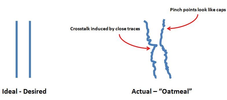
produce non-uniform routes. For high-speed I/O routes within the chip, this can
metaphorically look like this:
The ultimate result is that process variation
can have a significant impact across a wafer, and across the die based upon their
size. And with the geometries being so small, effects such as propagation
delay, crosstalk and current leakage are much more pronounced; so more rigor in
PVT (Process/ Voltage/ Temperature) testing must be taken. So a 5X5 testing methodology (five tests on five systems, each with different chips)
is the minimum necessary to establish confidence in design margins.


