Our chief technologist of non-intrusive board test, Adam
Ley, recently published an e-Book
on solving the problem of diminishing test coverage from In-Circuit Test (ICT).
What’s the key take-away from this publication?
If you know Adam Ley, you know that he knows his stuff. He’s
had an active role in all things JTAG over the last 15 years, having
participated in virtually every related standard, including IEEE 1149.1,
1149.4, 1149.5, 1149.6, 1149.7, 1500, 1532, 1581, P1149.1.1, and P1149.8.1; not
to mention his contributions to industry forums such as iNEMI, PICMG, and
SJTAG. When Adam writes on a topic, you know that it’s well thought-out and
comprehensive.
In his e-Book, Adam covers some of the well-known technical
issues with ICT, such as increasing circuit density, problems from board
strain, EMI, and via stubs’ impact on high-speed I/O. A brief look at the
economics of ICT versus its software-based alternative, non-intrusive board
test (NBT), is accompanied by a technical overview of the latter’s fusion of
structural, functional and performance-based test technologies.
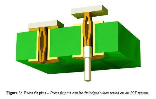
One of my favorite examples in the paper references the
negative impact that ICT test probes can have on press-fit connectors such as
DIMM or PCI Express. In the figure below, the counterforce exerted by the test
probe loosens or even dislodges the press-fit pin from the circuit board. This
can have a horrible effect on system signal integrity, performance and
operation.


