
Although it has been in the news for quite a while, one of the methods thought to be the way to extend Moore’s Law is finally reaching the point where it may be deployed in the near future — 3D Silicon Integration…
3D Silicon Integration is different from 3D Packaging in that 3D Packaging involves whole packaged chips and each chip can still be tested individually at wafer test, before and after packaging, and before and after integration into a complex chip assembly.
Largely, methods used to test, debug, and verify Multi-Chip Modules (MCM’s) are extensible into the 3D Packaging space. However, 3D Silicon Integration is the direct stacking of die on top of each other using Through-Silicon-Vias (TSV’s) or die stacking through the use of Silicon Interposers (a silicon die with just internal routing and external connection bumps) to align the TSV’s on one die to the TSV’s on another die. For 3D Integration, the TSV’s can be made with a technique known as “Drill and Fill” where a laser drills a hole and then the hole is filled with metal and bumped on both ends; or TSV’s can be made as connections to the top or bottom of a die with normal nanometer-scale chip logic and metal routing connected within the die. The TSV manufacturing process is a very stressful and potentially destructive process that includes wafer-thinning, back-grinding, and laser-drilling.
3D Silicon Integration: how will it stack up?
The current use model for 3D Integration seems to support three basic stacking formulas:
- The redesign of a legacy 2D chip or a brand new design into a 3D chip that is completely owned by one organization or company — so the placement of between chip interconnect TSV’s can be designed with the normal chip layout process and test and debug features are an extension of those in a 2D design.
- The stacking of multiple “homogeneous die” such as memory or microprocessors — where a single die created by a single organization or company can be designed to be stacked and each die is exactly the same.
- The stacking of multiple “heterogeneous die” from different die providers — where each layer in a stack can be viewed as a competitive socket with multiple die-providers vying for the position and each die must meet some standard to seamlessly plug into the overall stack — note the die standard should support the re-use of die in any number of different die-stacks and in any location within a die-stack.
For the case of 3D Integration, the die used for the stacking are fundamentally different from the die used for 3D Packaging:
A BASE Die, the one that is designed to connect to the board or socket, is made very much like a 2D chip today with pin connections and probe pads, but must additionally be the source for all board-level signals, powers and grounds for the rest of the die in the stack.
An UPPER Die, any die above the base die, has only TSV connections on the bottom and maybe the top. This means that UPPER Die are fundamentally different in that they have no pad ring — and because of the size of the TSV’s (which may be anywhere from 30 microns down to less than 2 microns) and interconnect bumps (usually around 30 microns) there is not a lot of room for probe pads. This creates a problem testing the UPPER Die at wafer probe with the conventional thought process of probing hundreds of signals and providing hundreds of power and ground connections. In addition, the stacking of these sorts of die results in a structure that requires a mixture of IC test and Board test — the fault models are not just IC test stuck-ats and transitions and leakage, but now also incorporate the PCOLA/SOQ/FAM Board test concepts to identify that the die exists, is the correct die in the correct spot in the stack, that the die is oriented and aligned correctly, is receiving power, and that the interconnecting TSV’s don’t have opens and shorts, and so on.
Test and debug issues with 3D Silicon Integration
So, what are the test and debug problems with “3D Silicon Integration” that are different from both 2D Silicon or 3D Packaging? Obviously, the BASE Die is very much like a 2D Die or 2D Die used for 3D Packaging in that they have pins, probe pads, and these connections can be brought out to both the top and bottom of a package. The BASE Die for 3D Integration has the addition of bumped connections on top of the bare die to allow an UPPER die to be directly connected — so the main test and debug issues are the “number of” and the “location of” the TSV’s to be used to access the test and debug logic on the UPPER Die.
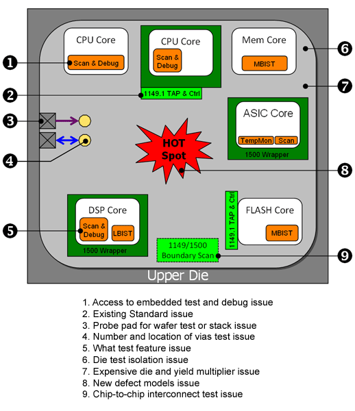
Figure 1: The extensive set of issues arising with 3D Silicon Integration
However, when we get to describing the test and debug issues, concerns, and problems with UPPER Die, the list grows significantly. There are the same concerns as with the BASE Die — how many TSV’s and where do you “physically” put them to allow the access mechanism to form just by stacking die?
And there are a number of other issues, as shown in figure 1. Since UPPER Die will most-likely have 100% of their signal and power & ground connections transferred through TSV-connections, and since TSV’s may be difficult to probe directly (and currently are not planned to have ESD protection), then there may not be any naturally existing “pads” that are usually used for wire bonding and probing. This leads to a similar question, “how many Probe Pads and where do you physically put them to enable bare-die or pre-bond test and debug?”
Once you solve the test and debug access problem, then the on-die embedded content issue arises in dealing with on-die cores and embedded instruments — what access architecture or access protocol is used if there may be logic representing IEEE Standards such as IEEE 1500, 1149.1, P1687, or 5001? And there may be a significant amount of embedded and doubly-embedded content such as Memory BIST, Logic BIST, MFG Scan, Debug and Trace, and Environmental Monitors: how are these resolved to die and eventually, stack connections?
Aside from what may exist due to legacy design or the application of existing standards, there may also need to be consideration of “new” on-die content to solve problems such as new defect models. One expected new issue is thermal hot spots on one die that can impact the die stack, or the cumulative impact of thermal hot spots on several die in the stack. New test content may be needed to enable true 3D test or debug by activating pattern generators, response evaluators, and control logic distributed throughout the stack. New features could be required to conduct die-to-die interconnect testing, especially if some of the interconnects between any given die are high-speed Gigabit signals.
Exponential reduction in stacked die yields
The concerns associated with any given UPPER Die, from a Stack or Stacking point of view, have to do with “yield and cost”. Similar to board test, most board assembly houses make a chip-assembly decision based on the cost of the chip — very inexpensive boards are tested before soldering very expensive chips to them to prevent having to discard (or rework) an expensive combination. Similarly, there will be decisions made to test inexpensive partial stacks before committing a very expensive die (for example, three 10 cent die can be stacked and tested before stacking a $4.00 die).
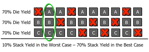
Figure 2: Accumulated yields for a stack of 3 die, each of which has a 70% yield
One of the other issues with stacking is the Yield-Loss multiplication problem, which is a real problem for wafer-on-wafer stacking where good die on one wafer map to bad die on another wafer. If a die stack is made of 3 different die and each die has a 90% yield rating, then it is expected for 1 in every 10 die to be bad. At the worst case, if the bad die are distributed across 10 assembled stacks, the overall stack yield could be 70% (three of the 10 stacks would have a bad die). If the stack was made of 5 different die, then it may be possible for 1 die in each die family to be bad — and a group of 10 stacks could have 5 bad die distributed, for a worst case overall stack yield as low as 50%. If there were 10 die in a stack, then similar math would show that overall stack yield could result in a 0% yield — that is with 90% individual die yield.
If the individual die yield was 70%, as shown in figure 2, then 3 out of 10 die would be bad, and the original 3 die stack could end up with 10% overall stack yield (9 bad die distributed in 10 stacks).
This means that Known-Good-Die (KGD) must be rigorously tested to achieve a very high delivered individual die yield — which requires the ability to comprehensively test at wafer or bare-die, and requires that in-stack testing will allow isolation to an individual die (or else, there will be no way to provide feedback to fix the yield-loss problem from the die-providers).
IEEE P1838 to the rescue
There are clearly a lot of issues above and beyond those associated with 2D chips — and some fairly complex issues. Because of the complexity, a solution isn’t as easy as a couple of chip design companies colluding to try to bend and apply existing standards (such as IEEE 1149.1). In view of this complexity, an IEEE Study Group spent much of 2010 evaluating the need for a new IEEE Standard.
In January of 2011, the P1838 Working Group started meeting to document the issues identified by the Study Group, turning them into requirements, and beginning the work of proposing a “per die” standard that would support access to, and operation of, test and debug logic associated with each die in all potential environments. This means that a standard access port and possibly access controller would be defined for each die so that individual die associated with 3D Silicon Integration could be tested or debugged at wafer probe and bare-die testing (pre-stacking); at partial stack assembly (mid-stacking); at whole stack (post-stacking); and at package, final, board, and system (post-packaging).
The IEEE P1838 Working Group is chaired by Erik Jan Marinissen of IMEC and co-chaired by Adam Cron of Synopsys. The secretary is Sophocles Metsis of AMD, and the two co-editors are Michael Wahl of the University of Siegen and Al Crouch of ASSET InterTech. There are currently 45 active members other than the officers and they represent about 30 different companies and universities. The meetings are held weekly on Thursdays at 8AM Pacific time.
To find out more just visit http://grouper.ieee.org/groups/1838/ or send email to me, Alfred Crouch: acrouch @ asset-intertech . com (remove the spaces).
You could also read my blog explaining how IEEE 1687 could be used in conjunction with IEEE P1838 to simplify its implementation.